Researchers report having exceeded a one-watt output power with a quantum cascade terahertz laser.
Terahertz waves, which lie in the part of the electromagnetic spectrum between infrared and microwaves, can penetrate materials that block visible light. They could potentially monitor pharmaceutical products, remotely sense chemical signatures of explosives in unopened envelopes, and non-invasively detect cancers in humans.
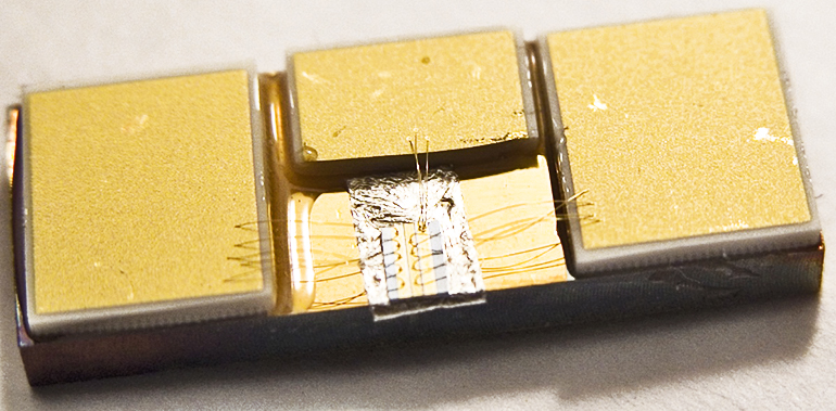
(Credit: University of Leeds)
However, one of the main challenges for scientists and engineers is making the lasers powerful and compact enough to be useful.
“Although it is possible to build large instruments that generate powerful beams of terahertz radiation, these instruments are only useful for a limited set of applications,” says Edmund Linfield, professor of terahertz electronics in the University of Leeds School of Electronic and Electrical Engineering.
“We need terahertz lasers that not only offer high power but are also portable and low cost.”
The quantum cascade terahertz lasers in development by Linfield and colleagues are only a few square millimeters in size.
In October 2013, Vienna University of Technology announced that its researchers had smashed the world record output power for quantum cascade terahertz lasers previously held by Massachusetts Institute of Technology (MIT).
The Austrian team reported an output of 0.47 watt from a single laser facet, nearly double the output power reported by the MIT team. The Leeds group has now achieved an output of more than one watt from a single laser facet.
“The process of making these lasers is extraordinarily delicate. Layers of different semiconductors such as gallium arsenide are built up one atomic monolayer at a time,” says Linfield.
“We control the thickness and composition of each individual layer very accurately and build up a semiconductor material of between typically 1,000 and 2,000 layers.”
The Engineering and Physical Sciences Research Council was the main source of funding for the research, which is published in Electronics Letters.
Source: University of Leeds
Article was originally published at www.futurity.org